Digital Inverter Rev04#
Changes from Rev03 production to Rev04#
Added separate gate resistors for turn-off (12 Ohm) and turn-on (47 Ohm) MOSFETs.
Introduced a new capacitor bank consisting of 8x AEC capacitors (110µF each) and 15x MLCCs (10µF each).
Added an individual 2.5V supply (REF4132B25DBVRQ1) as a bias reference for (ADA4940-1ARZ-R7 and INA241A2IDGKR).
Replaced Current Sense Amplifier (MAX40056TAUA+ ).
New current sensor makes hardware Over Current Protection obsolete.
Optimized the entire layer stackup and re-engineered the PCB layout.
Eliminated low-side temperature measurement from all phases.
Note
Moved the heatsink in Rev04 to the bottom of the PCB.
Components#
Additional to the components all version share, the following components are used:
Bi-directional current measurement INA241A2IDGKR
2.5V supply REF4132B25DBVRQ1
Absolute maximum ratings#
Warning
Current up to \(I_{peak}=\pm33.94\ A\) or \(I_{rms}=\pm24\ A\)
Voltage up to \(V_{peak}=48\ V\) or \(V_{rms}=33.94\ V\)
Operating temperature of the MOSFET \(T_{j,max}=175°C\)
Additional ratings#
Note
Current measurement up to \(I_{peak,meas}=\pm50\ A\)
Voltage measurement up to \(V_{peak,meas}= 60\ V\)
Temperature measurement up to \(T_{meas}=105°C\)
Temperature measurement is not built into the MOSFET. Therefore the heat of the PCB close to the semiconductors is measured. The measured temperature will always be significantly lower than the max operating temperature of the semiconductors.
DC-link capacitance \(C_{DC} = 1030\mu F\)
Cutoff frequency for voltage measurement \(f_g = 1745\ Hz\)
Operation up to a PWM frequency of \(f_{PWM} = 100\ kHz\) has been verified
Heatsink#
Rev04 requires a redesigned heatsink, which is not compatible with previous revisions Rev02 and Rev03. The PCB is prepared for the installation of a heat sink. Four mounting holes have been incorporated, designed to support screws with a maximum diameter corresponding to M3. It is intended that the heatsink will have the appropriate holes with threads into which the screws can be screwed. For further information on the dimensions of the heatsink and the location of the screw holes, refer to the diagram below. The dimensions take into account the safety margin required for the mounting rails in the UltraZohm. The heatsink is mounted on the bottom side of the PCB. Adequate mechanical clearance has been ensured to accommodate the heatsink within the designated space. A thermal interface material must be applied between the heatsink and the PCB to ensure optimal thermal conductivity.
Fig. 281 Heatsink dimensions
Pinout#
Adapter Card Pin |
Net Name |
Signal Description |
Signal Type |
Direction seen from Adapter Board |
|---|---|---|---|---|
DIG_IO_00 |
PWM H1# |
Gate H1 |
PWM/Direct |
Input |
DIG_IO_01 |
PWM L1# |
Gate L1 |
PWM/Direct |
Input |
DIG_IO_02 |
PWM H2# |
Gate H2 |
PWM/Direct |
Input |
DIG_IO_03 |
PWM L2# |
Gate L2 |
PWM/Direct |
Input |
DIG_IO_04 |
PWM H3# |
Gate H3 |
PWM/Direct |
Input |
DIG_IO_05 |
PWM L3# |
Gate L3 |
PWM/Direct |
Input |
DIG_IO_06 |
unused |
|||
DIG_IO_07 |
H1 Temp |
Temperature feedback H1 |
PWM |
Output |
DIG_IO_08 |
unused |
|||
DIG_IO_09 |
unused |
|||
DIG_IO_10 |
unused |
|||
DIG_IO_11 |
unused |
|||
DIG_IO_12 |
unused |
|||
DIG_IO_13 |
unused |
|||
DIG_IO_14 |
PWM EN |
Enable Gate signals |
Level, high active |
Input |
DIG_IO_15 |
unused |
|||
DIG_IO_16 |
unused |
|||
DIG_IO_17 |
OT H1 |
Fault indicator H1 |
Level, low active |
Output |
DIG_IO_18 |
H3 Temp |
Temperature feedback H3 |
PWM |
Output |
DIG_IO_19 |
H2 Temp |
Temperature feedback H2 |
PWM |
Output |
DIG_IO_20 |
unused |
|||
DIG_IO_21 |
unused |
|||
DIG_IO_22 |
unused |
|||
DIG_IO_23 |
unused |
|||
DIG_IO_24 |
unused |
|||
DIG_IO_25 |
unused |
|||
DIG_IO_26 |
unused |
|||
DIG_IO_27 |
unused |
|||
DIG_IO_28 |
OT H3 |
Over temperature indicator H3 |
Level, low active |
Output |
DIG_IO_29 |
OT H2 |
Over temperature indicator H2 |
Level, low active |
Output |
Compatibility#
This digital adapter inverter board is directly compatible with the Inverter Adapter IP core. It can be used in any of the D1-D4 digital adapter card slots in the UltraZohm, provided the correct CPLD is flashed. The card is directly compatible with the Analog LTC2311-16 Rev05 and Rev06, Analog LTC2311-16 3v01 and Analog LTC2311-16 2vXX cards.
Switching behavior#
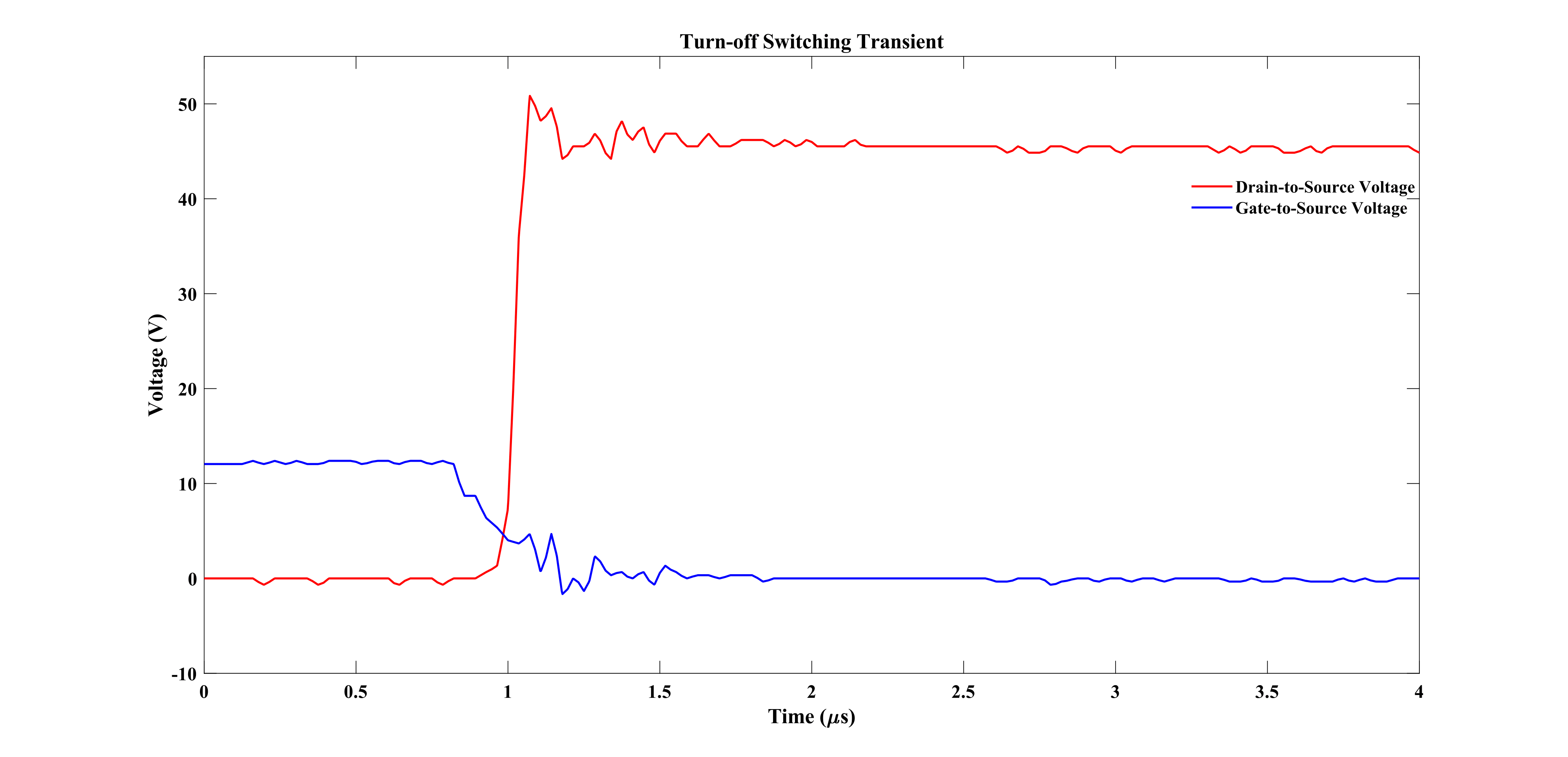
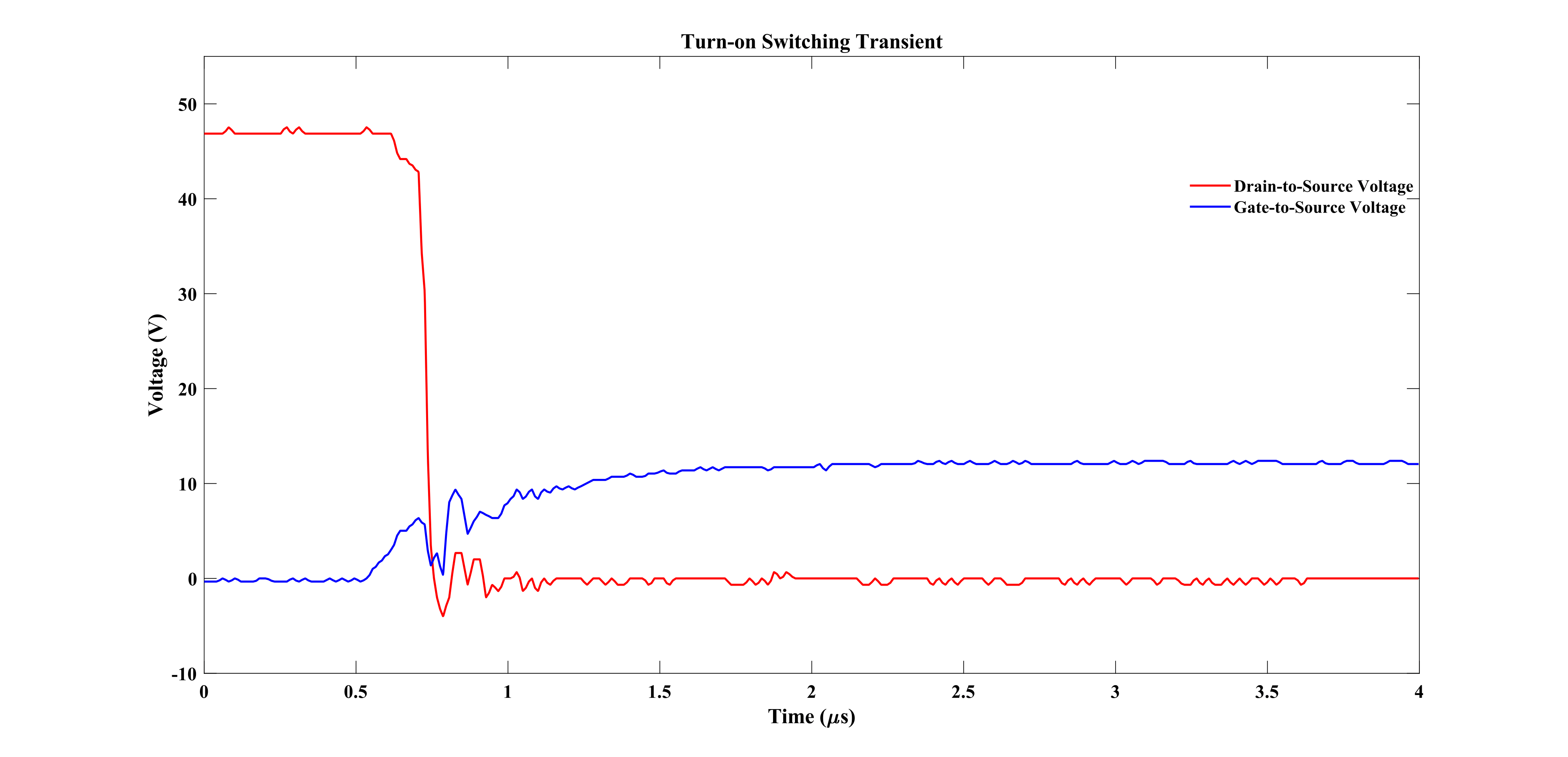
The Double Pulse Test (DPT) was used for characterizing the switching behavior of the design. The DC link voltage was set to \(V_{dc} = 48\ V\), with a load inductance of \(L = 1\ mH\) and a load resistance of \(R_L = 400\ mΩ\). The desired switching current was maintained at \(i_D = 30\ A\) throughout the test. The experimental waveforms of the DPT are shown below. One must note that, due to design constraints, measurement of the drain current was not included. The DC-Current at the negative terminal is therefore shown in the graph.
Setup before first use and implementation with Inverter Interface IP core#
CPLD#
Make sure that the correct CPLD is flashed in the corresponding digital adapter slot.
For this adapter card the uz_d_3ph_inverter CPLD needs to be flashed.
Download this CPLD from the UltraZohm CPLD Repository.
Follow this guide on how to flash the correct CPLD on the UltraZohm.
Software implementation#
This adapter card interacts with the user via the highly sophisticated Inverter Adapter IP core and its associated driver.
Follow this guide to integrate the IP core into the FPGA and to set up the software driver.
While following this guide, be sure to adjust the linear interpolation parameters for the inverter_adapter_config.
For this inverter card they should be:
.linear_interpolation_params = {-289.01f, 218.72f}
Set the deadtime in the uz_interlockDeadtime2L_staticAllocator.c file to an appropriate value.
A safe value with a considerable safety margin is 200ns.
No matter what, the deadtime should not be lower than 150ns.
uz_interlockDeadtime2L_staticAllocator.c file. Shown is an example for the D1 slot.#static uz_interlockDeadtime2L interlock_slotD1_pin_0_to_5 = {
.base_address = XPAR_UZ_DIGITAL_ADAPTER_D1_ADAPTER_GATES_UZ_INTERLOCKDEADTIME_0_BASEADDR,
.clock_frequency_MHz = 100,
.deadtime_us = 0.2,
.inverse_bottom_switch = false };
To enable or disable the PWM_EN for normal operation, add the following code to the isr.c.
It should always be ensured, that the PWM_EN is handled correctly.
I.e. if the UltraZohm transitions into its error-state e.g. because the OCP is triggered, it must be ensured, that the PWM_EN is retracted.
Pay attention to this during your error handling.
if (current_state == running_state || current_state == control_state) {
  // enable inverter adapter hardware
  uz_inverter_adapter_set_PWM_EN(Global_Data.objects.inverter_d1, true);
} else {
  // disable inverter adapter hardware
  uz_inverter_adapter_set_PWM_EN(Global_Data.objects.inverter_d1, false);
}
To read out the measured current and voltage signals, both Ethernet cables have to be connected to an ADC-Card.
In the isr.c add the following conversion factors to the measured signals.
struct uz_3ph_abc_t v_abc_Volts = {0};
struct uz_3ph_abc_t i_abc_Amps = {0};
float v_DC_Volts = 0.0f;
float i_DC_Amps = 0.0f;
v_abc_Volts.a = Global_Data.aa.A1.me.ADC_B8 * 12.0f;
v_abc_Volts.b = Global_Data.aa.A1.me.ADC_B7 * 12.0f;
v_abc_Volts.c = Global_Data.aa.A1.me.ADC_B6 * 12.0f;
v_DC_Volts = Global_Data.aa.A1.me.ADC_A1 * 12.0f;
i_abc_Amps.a = Global_Data.aa.A1.me.ADC_A4 * 12.5f;
i_abc_Amps.b = Global_Data.aa.A1.me.ADC_A3 * 12.5f;
i_abc_Amps.c = Global_Data.aa.A1.me.ADC_A2 * 12.5f;
i_DC_Amps = Global_Data.aa.A1.me.ADC_B5 * 12.5f;
Note
These are the theoretical conversion factors. They might differ slightly in reality do to component tolerances.
In order to use the over current and over temperature protection, the following code has to be added to the isr.c as well. These are optional features and can be left out if they aren’t required.
//Read out overtemperature signal (low-active) and disable PWM and set UltraZohm in error state
//Overtemperature for H1
if (!Global_Data.av.inverter_outputs_d1.FAULT_H1) {
   ultrazohm_state_machine_set_error(true);
}
//Overtemperature for H2
if (!Global_Data.av.inverter_outputs_d1.FAULT_H2) {
   ultrazohm_state_machine_set_error(true);
}
//Overtemperature for H3
if (!Global_Data.av.inverter_outputs_d1.FAULT_H3) {
   ultrazohm_state_machine_set_error(true);
}
References#
Known issues#
As of this moment, no issue in Rev04 is known.
Designed by#
Krunal Patel/ Dennis Hufnagel (THN), 06/2025
Acknowledgments#
Special thank you for their support during the design and testing phase goes to Eyke Aufderheide (TUM), Michael Hoerner (THN) and Tobias Schindler (THN).