Create a CPLD program using ABEL#
The main goal of this section is to describe the necessary steps for creating a simple program for the
ispMACH LA4128V or LC4256V CPLDs on the UltraZohm \(\leq\) Rev04.
All signals from the FPGA to the digital adapter cards have to pass through the CPLDs.
Everything is programmed inside the .abl file. Here we can set which ports are inputs or outputs and use logic combinations to create the desired behavior.
Step-by-step#
Install the ispLEVER Classic software from Lattice and clone the CPLD repository, see Install Lattice Toolchain (CPLD) for details.
Create a new branch in the repository, e.g.
feature/project_name.Inside the CPLD repository
ispMACH/LA4128V/orispMACH/LC4256V/, create a copy of an existing project folder, e.g.optical_14tx_4rx.Rename the folder to your project name, try to use a meaningful name.
Delete all HTML and JED files from your project folder. Only
top_level.ablandoptical_14tx_4rx.synshould be left.Rename the project file to match your project folder name:
uz_cpld_project_name.syn.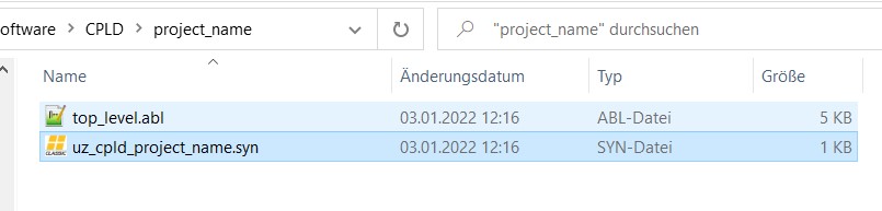
Open the top_level.abl file. In the beginning, all pins are defined and assigned to a physical pin on the CPLD.
fpga_00..fpga_29pins are connected to the FPGA/Zynq UltraScale+d_00..d_29pins are connected to the digital adapter
The numbering is zero-based and equivalent to the one in Vivado and in the Altium schematics of the Carrier Board and the Digital Adapter Cards. Do not change this part. It is the same in all projects.
" PIN ASSIGNMENTS
" FPGA pins
fpga_00 pin 3;
...
fpga_29 pin 98;

" Digital Adapter pins
d_00 pin 50;
...
d_29 pin 70;
At the end of the file, there is the section that defines the logic. In the simplest case, this is just an assignment, in the example below
fpga_00is an input and assigned to the outputd_00, and vice-versa for pinsd_29andfpga_29.EQUATIONS d_00 = fpga_00; fpga_29 = d_29;
It is also possible to create combinational logic of multiple inputs. The word
nodeis an ABEL keyword and creates a signal. This can simplify the logic. The compiler will usually resolve those signals to a combination of inputs only. In the example below, the output is enabled iffpga_26andfpga_27are 0, whilefpga_28andfpga_29are 1.enable_signal node; EQUATIONS enable_signal = !fpga_26 & !fpga_27 & fpga_28 & fpga_29; d_11 = fpga_11 & enable_signal;
Use the following logic to create an interlocking functionality, e.g. for the upper and lower switch of a half-bridge. In this case, the output
d_00is high whenfpga_00 = 1andfpga_01 = 0d_00is low in all other cases, e.g. iffpga_00 = 1andfpga_01 = 1
EQUATIONS
d_00 = fpga_00 & !fpga_01;
d_01 = fpga_01 & !fpga_00;
Now, open the project file
uz_cpld_project_name.synwith ispLEVER Classic and double-click on JEDEC File to create the bitstream for the CPLD.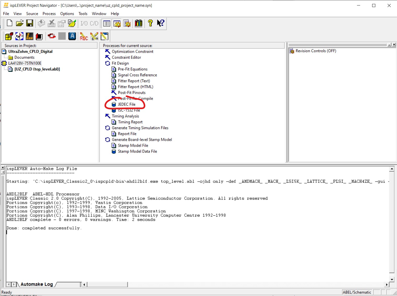
ispLEVER will prompt you asking which constraints to use. Simply press
Importto import them from thetop_level.ablfile.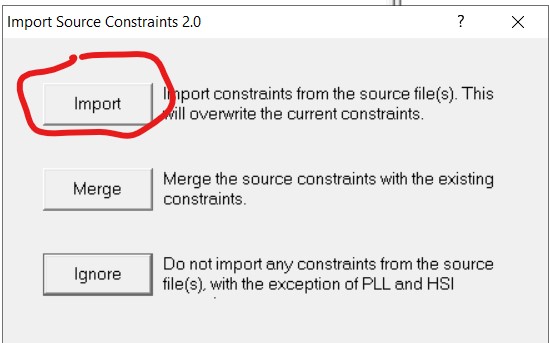
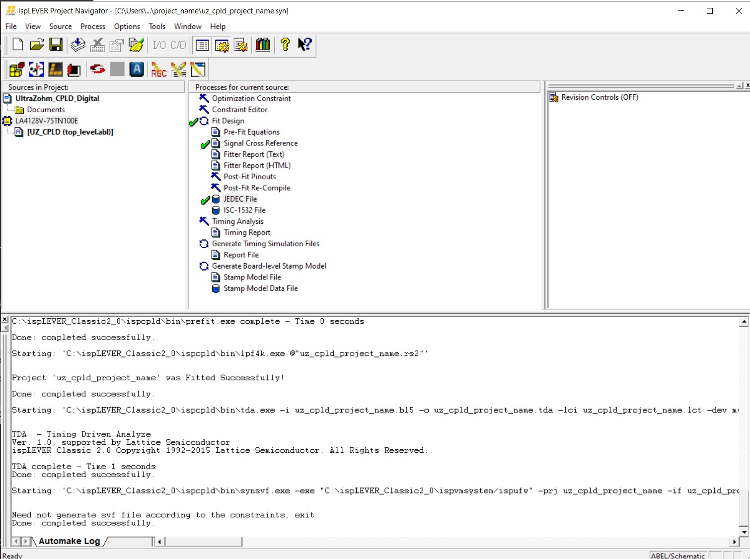
After successful compilation, it should look like this.
The folder is quite cluttered now, but we only track the highlighted files in git, i.e.
top_level.abl(main source file, including constraints and logic)uz_cpld_project_name.syn(project file)uz_cpld_project_name.html(report)uz_cpld_project_name_rpt.html(report)uz_cpld_project_name_toc.html(report)uz_cpld_project_name.jed(CPLD bitstream)
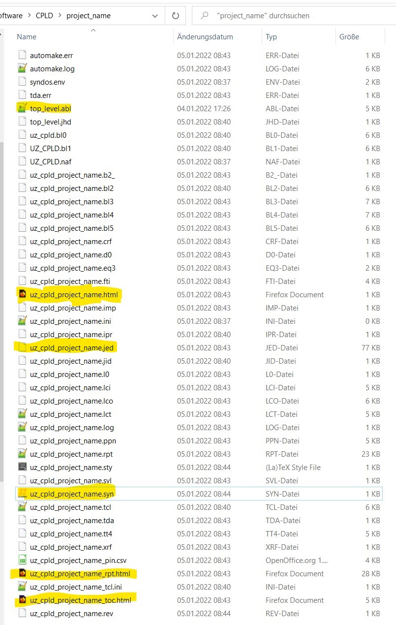
The file
uz_cpld_project_name.htmlcontains the documentation of the created CPLD program and includes a summary of all settings, e.g., which pin is an input or an output.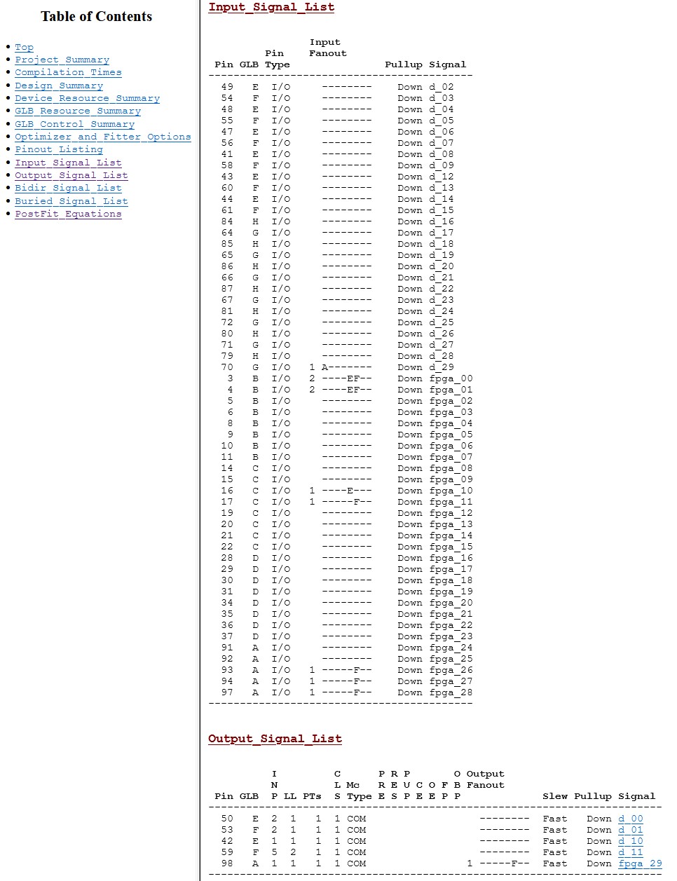
The report also includes the resulting equations under the tab PostFit_Equations. As mentioned above, the
enable_signalwas resolved into a combination of input pins.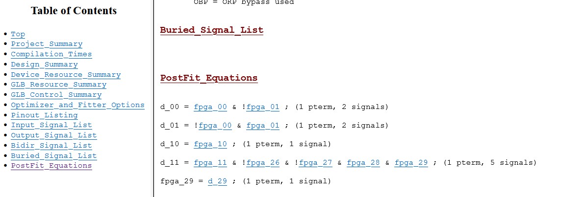
If the report matches the expected outcome, the job in ispLEVER is done. You can program the CPLD as described in Programming the CPLD.
After testing it on the UltraZohm, commit your new or modified project to the git repository and open a pull request.