Wolfspeed Inverter 2L 25 kW Interface Rev04#
Rev04 is the second productive revision of the uz_per_wolfspeed_25kw_FM3 interface PCB.
Rev04 keeps the analog measurement concept of Rev03 and adds several digital functions for commissioning and inverter operation.
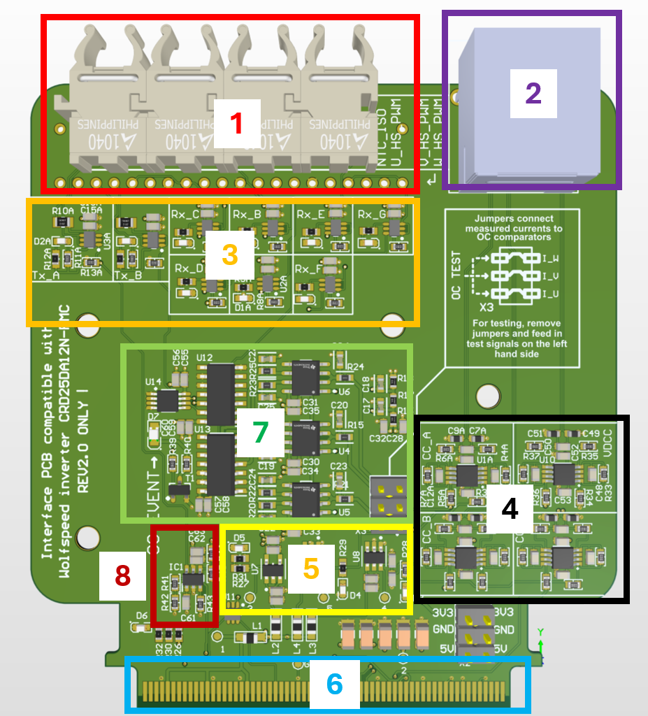
Fig. 307 Functional areas of the Rev04 interface PCB.#
The PCB is structured by functional areas as shown in Functional areas of the Rev03 interface PCB with:
HFBR-1521Z/2521Z digital optical transmitters and receivers
RJ45 port for analog signal transmission
Driver stages for the optical links
TI THS4561 fully differential amplifier stages
Power supply with TPS7A20 3.3 V LDO and REF35 voltage references
Samtec HSEC8 120-pin edge-card connector mating with the Wolfspeed inverter
Window comparators, AND gates, and flip-flop for overcurrent detection and latch
LTC6992 analog NTC temperature to PWM conversion
Changes Compared to Rev03#
Added
GateAndFanControl.SchDoc:Gate_Driver_Enableis converted to the inverterGD_DISpolarity and also drives the fan-control output.Added
OvercurrentDetectionLogic.SchDoc: the six overcurrent comparator outputs are combined, latched, reset by gate enable, and routed to the opticalOCoutput.Added
TempSenseConditioning.SchDoc: the analog isolated NTC signal is converted to a PWM signal before the optical transmitter.Added fan outputs
FAN1_OUTandFAN2_OUTon the inverter connector.Added a red overcurrent latch indicator LED.
Added a 2x3 jumper header in the overcurrent section for testing overcurrent events.
Analog Signals#
Rev04 keeps the Rev03 analog measurement structure. The inverter-side phase-current and DC-link voltage measurements are converted from single-ended signals to fully differential signals for the UltraZohm ADC board.
Signal |
Source |
Total measurement gain |
UltraZohm ADC channel |
|---|---|---|---|
Phase current U |
LEM LAH 50-P |
0.03993 V/A, bandwidth about 50 kHz |
|
Phase current V |
LEM LAH 50-P |
0.03993 V/A, bandwidth about 50 kHz |
|
Phase current W |
LEM LAH 50-P |
0.03993 V/A, bandwidth about 50 kHz |
|
DC-link voltage |
Non-isolated voltage divider |
0.003744 Vsec/Vprim, bandwidth about 7 kHz |
|
Digital Signals#
Signal |
Direction |
Conditioning |
Notes |
|---|---|---|---|
|
UltraZohm to inverter |
Optical receivers |
High-side and low-side PWM for three phases; dead time is generated in the UltraZohm. |
|
UltraZohm to interface |
Optical receiver, then inverter logic |
High enables the gate drivers and arms overcurrent protection. |
|
Interface to inverter |
Derived from |
Fans are on when |
|
Interface to UltraZohm |
SN74HCS08DR logic, SN74LVC1G74 latch, optical transmitter |
Combined and latched overcurrent feedback. The latch clears when |
|
Interface to UltraZohm |
LTC6992CS6-2 PWM generator and optical transmitter |
PWM representation of the isolated NTC voltage. |
Warning
The printed label on the PCB called GD_DIS for the optical receiver is wrong.
Actually this is Gate_Driver_Enable, a high-active enable signal.
Gate Enable and Fan Control#
Rev04 separates the UltraZohm-side gate-enable command from the inverter-side disable polarity. The schematic states the following behavior:
|
Resulting output |
Function |
|---|---|---|
High |
|
Gate drivers enabled, fans on, overcurrent protection armed. |
Low |
|
Gate drivers disabled, fans off, overcurrent latch cleared. |
Overcurrent Detection#
The Rev04 overcurrent (OC) detection uses TLV3502 comparators for the three phase-leg overcurrent signals:
U_HI_OC, U_LO_OC, V_HI_OC, V_LO_OC, W_HI_OC and W_LO_OC.
The comparator outputs are combined with SN74HCS08DR logic.
The result is latched with an SN74LVC1G74 flip-flop and routed to the OC optical transmitter.
When the gates are enabled, protection is armed.
When the gates are disabled, the latch is cleared.
The optical OC signal is high when an overcurrent event has been detected, which latches the signal.
The inverter gates are disabled until the OC latch is reset via a low signal on Gate_Driver_Enable.
Disabling the gate signals is independents of an active Gate_Driver_Enable signal.
The OC trips at +/-49 A.
Note
Rev04 includes a 2x3 jumper header in the overcurrent section for testing overcurrent events. For normal operation, i.e., an active overcurrent detection, place the jumpers as stated in the explanatory figure, connecting left and right pins of each row.
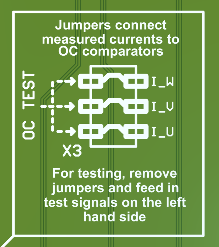
Fig. 308 Jumper setup for overcurrent comparators.#
NTC_ISO conversion for inverter V2.0#
For the CRD25DA12N-FMC V2.0 inverter and adapter Rev04, the signal chain is NTC -> analog
NTC_ISO -> 1:2 adapter voltage divider -> LTC6992-2 -> optical Temp_PWM -> duty ratio.
The LTC6992-2 is configured with:
R_SET = 68 kOhm, resulting in an approximately46 kHzPWM frequency.DIVCODE = 2/N_DIV = 16, selected by the182 kOhmand976 kOhmdivider.POL = 1, so increasing NTC temperature results in increasing duty cycle.
On the inverter, the NTC is in parallel with \(1.8\,\mathrm{k\Omega}\); this combination and \(2.2\,\mathrm{k\Omega}\) form a divider supplied by \(5\,\mathrm{V}\). Consequently,
The adapter and LTC6992-2 transfer functions are
where \(D\) is a ratio from 0.0 to 1.0. Thus,
Using the WolfPACK NTC approximation \(R_{25}=5\,\mathrm{k\Omega}\) and \(\beta_{25/100}\approx3523\,\mathrm{K}\), the temperature follows from
Clamp behavior#
The LTC6992-2 clamps its PWM output outside the nominal 5 % to 95 % duty-cycle range.
Below or above these limits the PWM does not contain an unambiguous temperature. The lower clamp
corresponds to approximately \(T\leq36.6\,{}^\circ\mathrm{C}\) and the upper clamp to
\(T\geq154.1\,{}^\circ\mathrm{C}\). The implementation returns these boundary values instead
of extrapolating outside the valid range.
Duty ratio |
Duty cycle |
Approximate temperature in \({}^\circ\mathrm{C}\) |
|---|---|---|
\(D \leq 0.05\) |
\(\leq 5\,\%\) |
\(\leq 36.6\); lower clamp |
0.10 |
10 % |
42 |
0.20 |
20 % |
52 |
0.30 |
30 % |
61 |
0.40 |
40 % |
70 |
0.50 |
50 % |
81 |
0.60 |
60 % |
91 |
0.70 |
70 % |
103 |
0.80 |
80 % |
119 |
0.90 |
90 % |
140 |
\(D \geq 0.95\) |
\(\geq 95\,\%\) |
\(\geq 154.1\); upper clamp |
Conversion code#
#include <math.h>
#include "../include/wolfspeed_inverter_temperature.h"
#include "../uz/uz_HAL.h"

float wolfspeed_inverter_temperature_from_duty_ratio(float duty_ratio)
{
    uz_assert(duty_ratio >= 0.0f);
    uz_assert(duty_ratio <= 1.0f);

    const float duty_min = 0.05f;
    const float duty_max = 0.95f;
    if (duty_ratio <= duty_min)
    {
        return 36.6f;
    }
    if (duty_ratio >= duty_max)
    {
        return 154.1f;
    }

    const float v_ntc_iso = 1.8f - 1.6f * duty_ratio;
    const float r_ntc_ohm =
        (3960.0f * v_ntc_iso) / (9.0f - 4.0f * v_ntc_iso);

    const float r_25_ohm = 5000.0f;
    const float beta_K = 3523.0f;
    const float t_25_K = 298.15f;
    const float inverse_temperature_K =
        (1.0f / t_25_K)
        + (logf(r_ntc_ohm / r_25_ohm) / beta_K);

    const float temperature_K = 1.0f / inverse_temperature_K;
    return temperature_K - 273.15f;
}
The following application call has not yet been merged:
float const temperature_duty_ratio =
    uz_PWM_duty_freq_detection_get_duty_cycle_in_percent(
        Global_Data.objects.inverter_temperature_pwm);
Global_Data.av.inverter_temperature_pwm_duty_cycle_percent =
    temperature_duty_ratio * 100.0f;
Global_Data.av.inverter_temperature_pwm_frequency_Hz =
    uz_PWM_duty_freq_detection_get_frequency_in_Hz(
        Global_Data.objects.inverter_temperature_pwm);
Global_Data.av.inverter_temperature_degC =
    wolfspeed_inverter_temperature_from_duty_ratio(temperature_duty_ratio);
Note
Despite the API name uz_PWM_duty_freq_detection_get_duty_cycle_in_percent, the conversion
expects a ratio from 0.0 to 1.0. The example therefore multiplies the result by 100.0f
only when writing the _percent application variable.
Commissioning Notes#
Before first operation:
Mount the interface PCB with the two mentioned 3d-printed clamps tightly to the inverter. The .STL parts are available in the PCB-repository.
Check fan behavior before applying high DC-link voltage.
Verify the temperature PWM duty-cycle interpretation in the software or FPGA logic.
Check the overcurrent test jumper setting. Three jumpers need to be placed in order to set the OC detection active.
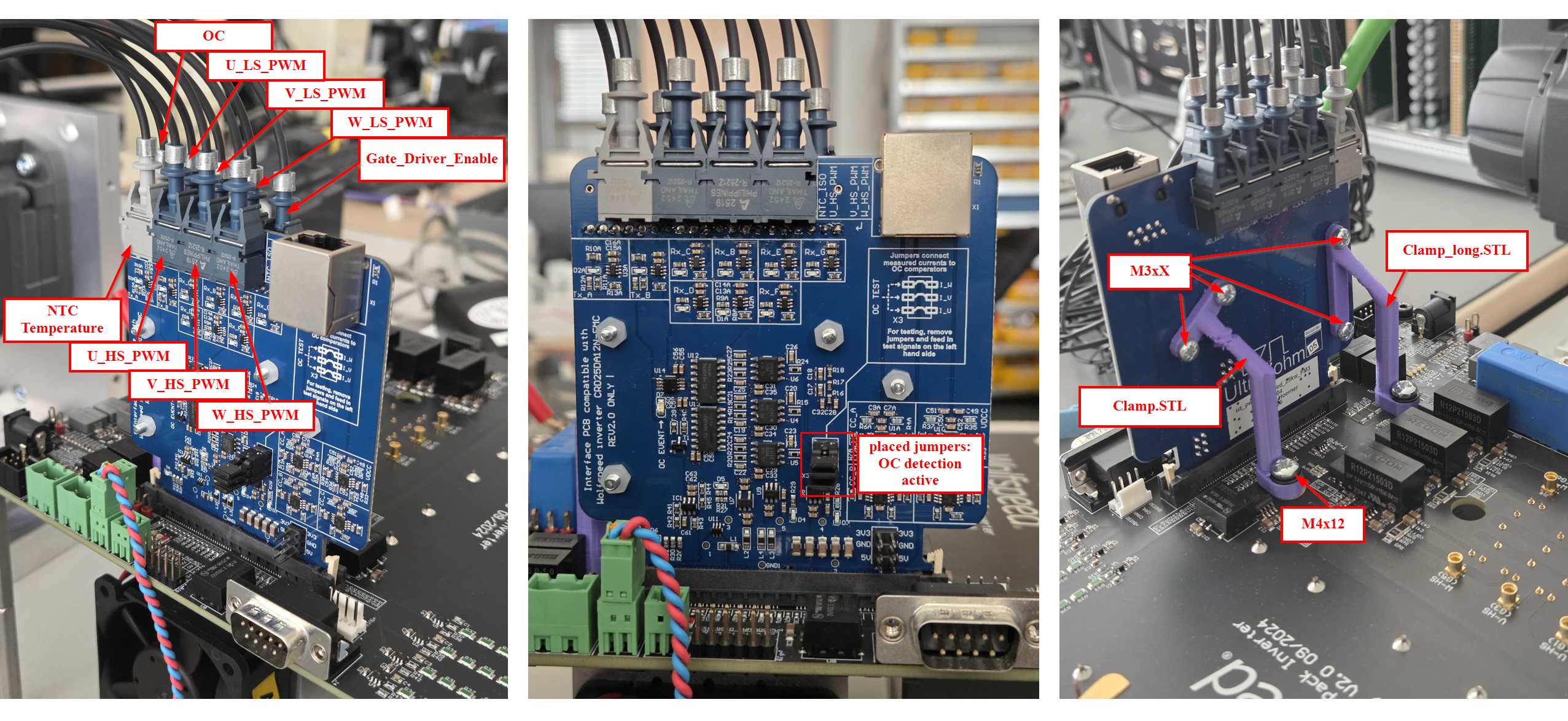
Fig. 309 Commissioning of the interface PCB with optical signal connections, mechanical mounting, and active OC circuitry#
Known issues#
The printed label on the PCB called
GD_DISfor the optical receiver is wrong. Actually this isGate_Driver_Enable, a high-active enable signal.